Frontier Global Applications of Monocrystalline Tungsten. AI-driven tungsten single crystal optimization. Advanced materials engineering for superior performance and efficiency.
1. Nanomaterial Analysis:
- Covers the entire process of metal ore extraction, smelting, and production.
- Involves biological, life sciences, medical and pharmaceutical applications, including non-destructive X-ray detection.
- Full-process analysis of plant production and organic materials, encompassing comprehensive material analysis, including field emission unit needles.
Approximately 200,000 high-magnification electron microscopes are deployed in global factories, research institutes, universities, and hospitals. These microscopes are replaced every two years, consuming about 100,000 tungsten needles annually. With an average price of $1,000 USD per needle, the annual market value reaches $100 million USD.
2. Semiconductor Consumables: New Energy, Batteries, 5G Stations, Energy Storage Products
In China, annual consumption is 100 million units; globally, 2 billion units. Currently, the entire industry uses ordinary metal materials at an average unit price of $1 USD, resulting in a total market size of $2 billion USD.
3. Core Chip Manufacturing Consumables (Key Testing Materials)
TSMC (Taiwan Semiconductor Manufacturing Company) consumes approximately 140,000 units per day (14 specifications, 10,000 units each). At an average unit price of $30 USD, the daily consumption value is $4.2 million USD, totaling approximately $1.533 billion USD annually.
4. These markets have only emerged in the past two years due to new high-end applications. With the rapid advancement of science and technology, these products are expected to experience exponential growth in demand annually.
Comparative Advantages of Our Company
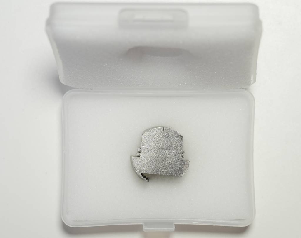
1. Field Emission Unit Needles
Currently, only the United States and Germany are capable of mass production. Our company in China has also achieved this capability.
Our product demonstrates an efficiency of over 70%, while those from the U.S. and Germany achieve approximately 50% efficiency.
2. TSMC High-Precision Tungsten Probe
Currently, Japan holds a monopoly in this sector. However, our company has mastered the complete production technology.
Our production costs are more than 80% lower than Japan’s, roughly 10% of the Japanese product cost, and we possess mass production capability.
We are scheduled to deliver final product samples to TSMC in September.

Special Notes:
The U.S. and Germany only possess the raw materials but cannot process them into final products with 0.005 mm tip precision (zero linear and curvature deviation).
Japan lacks the raw materials and only holds manufacturing technology.
Strategic Application:
- In high-end semiconductor chip manufacturing and nanomaterial research at million-times magnification, China-made products will achieve independent global leadership.
- Our products will enable technological independence and leadership in China’s aerospace and defense equipment sectors.
If you take interested in this, please contact +86 17171781717